Changelog
The first production LimeSDR XTRX was revision v1.2 and so this changelog starts with changes from that point.
Note
Details of internal-only versions which were never released are not included here.
v1.3
The reference clock structure was changed, replacing the separate general-purpose buffers with one dedicated clock buffer.
Added the ability to provide an external 3.3V supply, bypassing the switching regulators.
Various other small changes. See below for details.
RF Transceiver
A single clock signal (LMS_CLK) for both TX and RX PLLs was replaced by two separate clock signals, LMS_TxPLL_CLK for the TX PLL and LMS_RxPLL_CLK for the RX PLL.
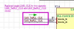
Figure 1. Separated LMS7002M RX and TX PLLs clocks schematics
Clock
Clock buffer updated and XO DAC changed.
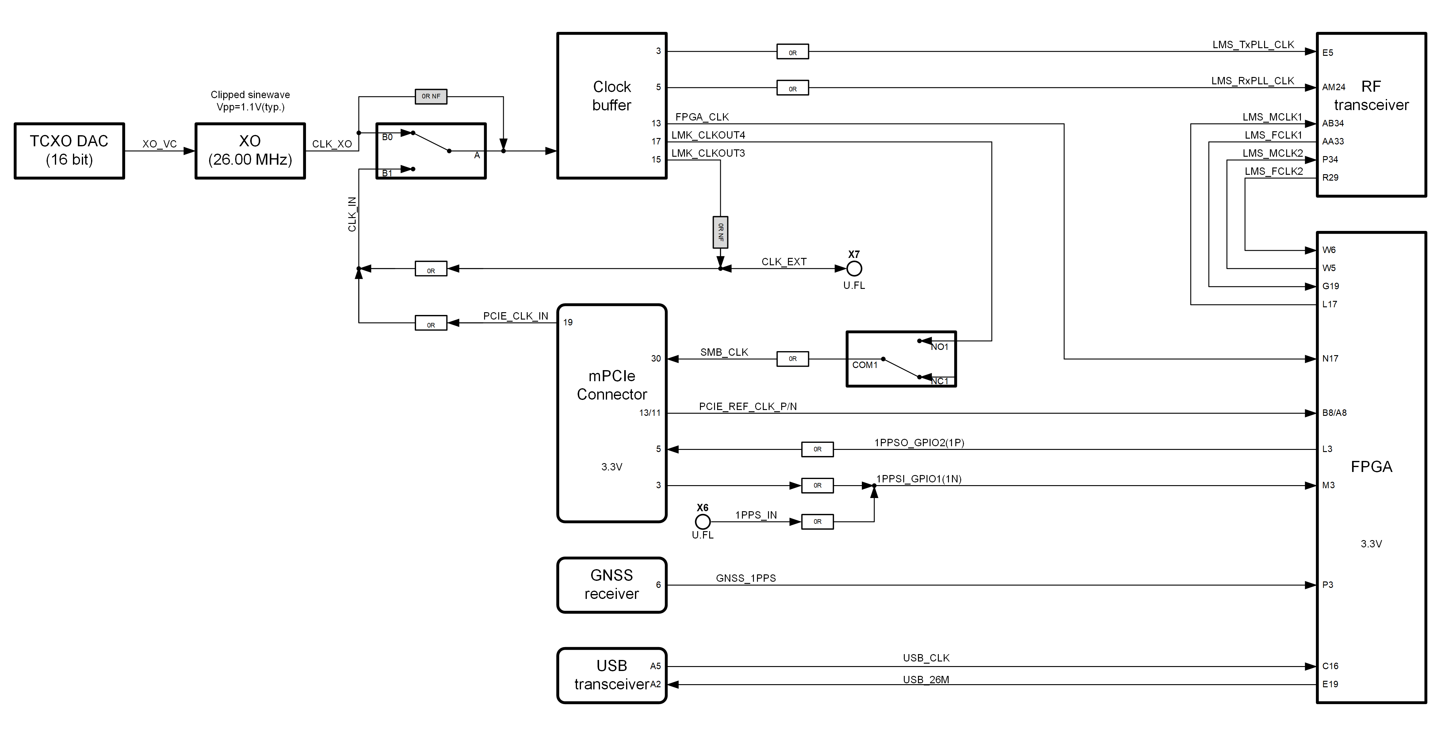
Figure 2. Clock block diagram
The new clock buffer is LMK00105. It generates clock signals in 1.8V and 3.3V logic. LMK00105 schematics are given in Figure 15.
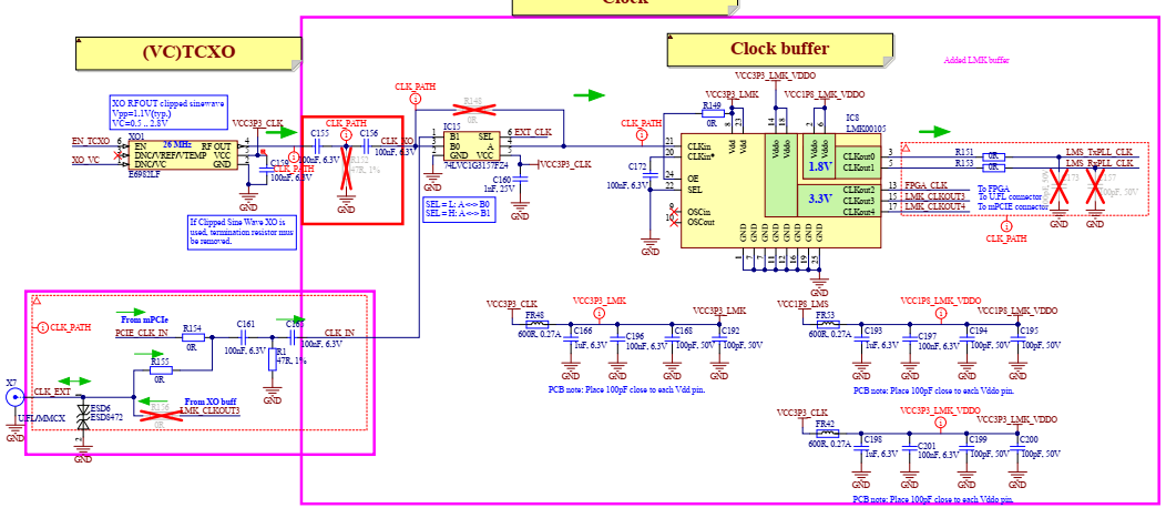
Figure 3. LMK00105 clock buffer schematics
Changed XO DAC from AD5693RACPZ-1RL7 (A grade, INL +-8LSB, internal reference, VLOGIC) to AD5693BCPZ-RL7 (B grade, INL +-3LSB, no internal reference, LDAC). Also removed R69, and populated R68 to tie LDAC pin low, so that the DAC updates when new data is written to the input register. XO DAC schematic changes are shown in Figure 16.
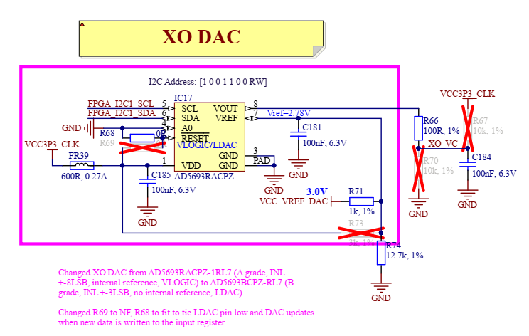
Figure 4. XO DAC changes
Power
It is now possible to connect VCC_EXT directly to VCC3P3 and VCC_CLK accordingly.
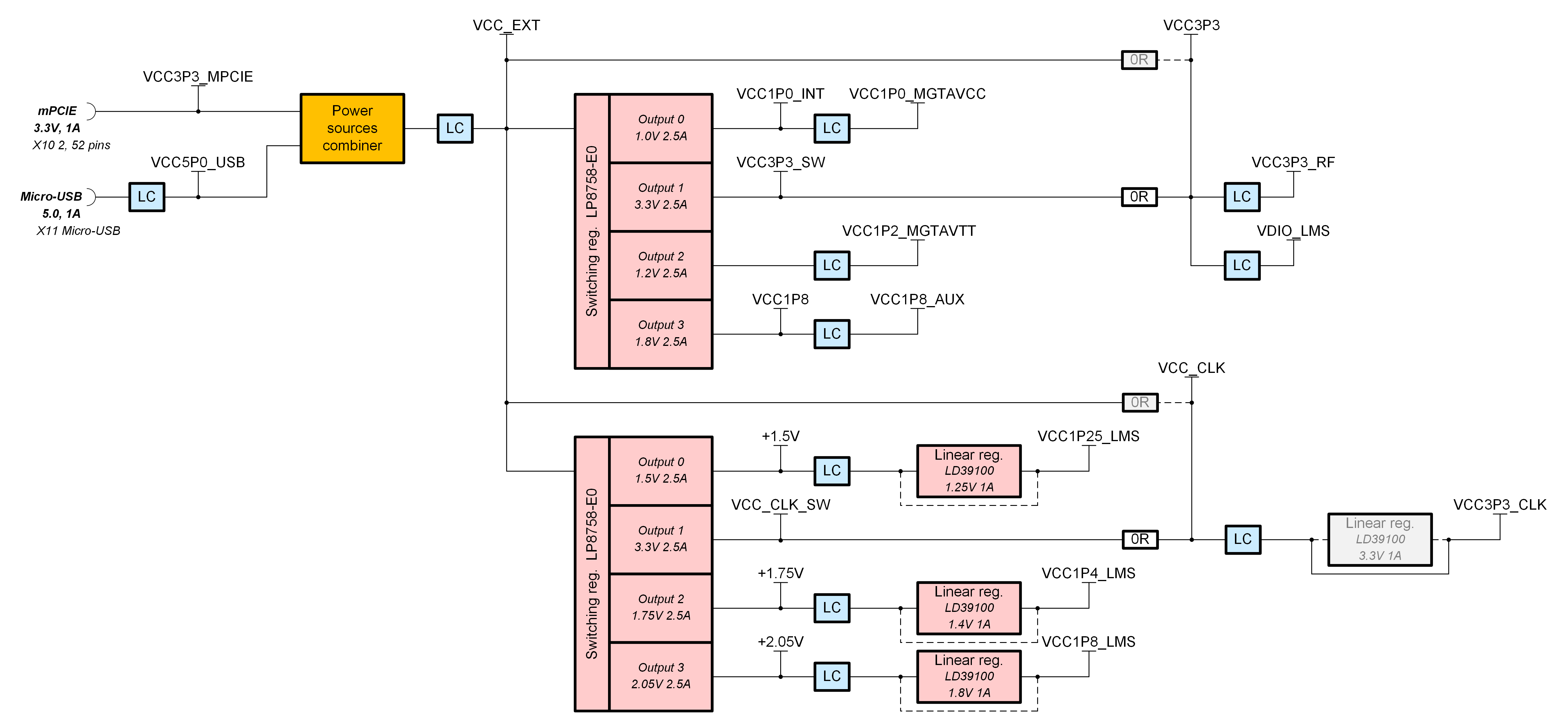
Figure 5. Clock power distribution
3.3 V Power signals generated by switching regulators were renamed from VCC3P3 to VCC3P3_SW and VCC_CLK to VCC_CLK_SW. And now can be disconnected from the main VCC3P3 and VCC_CLK power signals by removing R201 and R202.
Also removed VCC1P8_CLK power net and inductor. All switching regulator schematic changes are shown below.
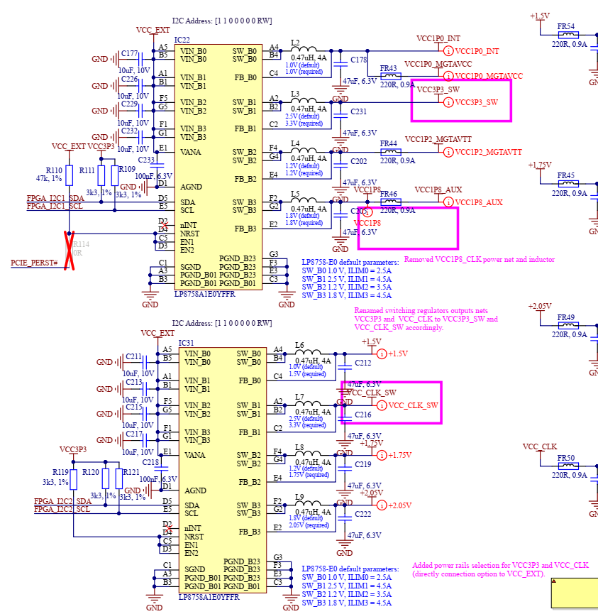
Figure 6. Switching regulators changes
Added power rails source selection for VCC3P3 and VCC_CLK. By default switching regulator outputs are selected as source (R201, R202 are populated and R198, R199 are remove) as shown in Figure 19.
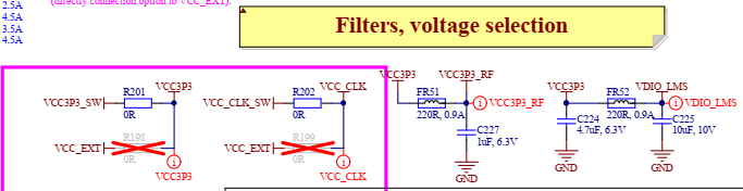
Figure 7. Power source selection
Miscellaneous
To make schematic signal naming more consistent, the PCIE_CLK_IN signal name was added to mPCIe connector (X10) pin 19. Also CLK_OUT signal name was changed to LMK_CLKOUT4, due to changes in the clock network described above.
PCIE_PERST# signals pulldown resistor (R90) was removed from schematics.
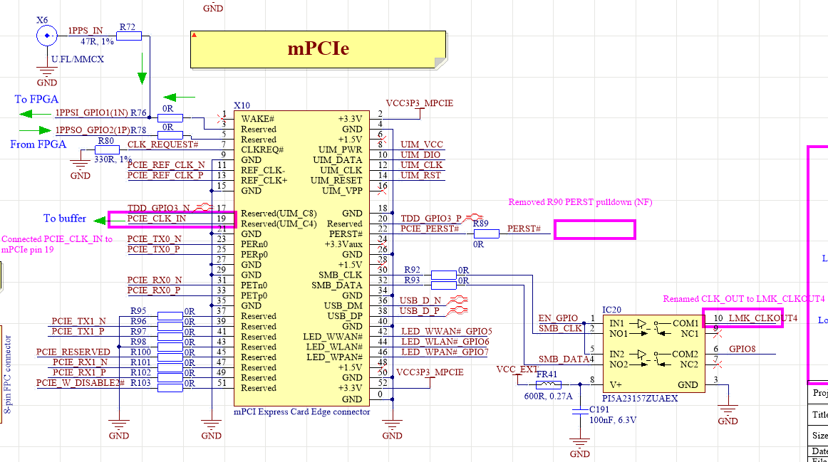
Figure 8. mPCIe connector changes
To make schematics easier to read the mechanical components shown below were moved from 05_LMS7002M_RF sheet to 09_Misc sheet.
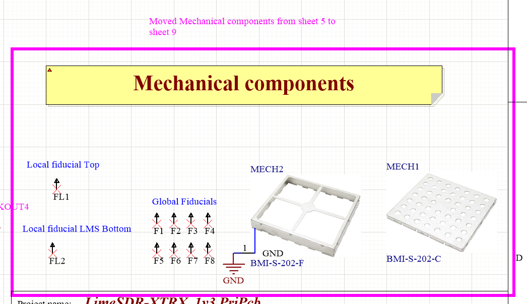
Figure 9. Mechanical components
Hardware and BOM Versions
The hardware version (HW_VER) was increased from 2 to 3, to allow software to automatically ascertain the board version. In addition to which the bill of materials version (BOM_VER) was reverted from 1 back to 0 (populated R49), to indicate that this is the original LimeSDR XTRX v1.3 build.
New BOM_VER and HW_VER schematics are given in Figure 11.
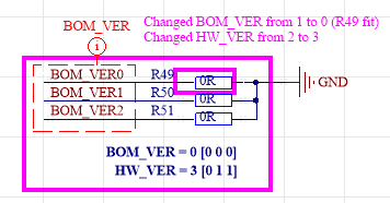
Figure 10. FPGA BOM_VER and HW_VER schematics changes
v1.2
First production version.